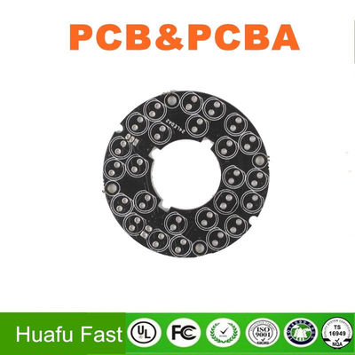
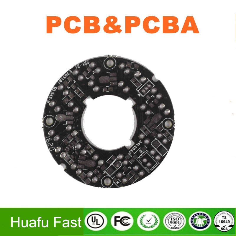
94V0 Copper Bare Single Sided PCB Board Manufacturing Black 1 Layer
Product Details:
| Place of Origin: | China |
| Brand Name: | HF |
| Certification: | ISO CE |
| Model Number: | Single Sided PCB |
Payment & Shipping Terms:
| Minimum Order Quantity: | 5PCS |
|---|---|
| Price: | Negotiable |
| Packaging Details: | High quality carton packing, high quality vacuum packing, |
| Delivery Time: | 5~8 days |
| Payment Terms: | L/C, T/T,PAYPAL |
| Supply Ability: | Ten thousand square meters per month |
|
Detail Information |
|||
| Base Material: | 94V0 | Layer Count: | 1 Layer |
|---|---|---|---|
| Board Thickness: | 1 Mm | Copper Thickness: | 1oz |
| Solder Color: | Black | Silkscreen Color: | White |
| Surface Finishing: | Osp | Service: | One Stop Turnkey Service |
| High Light: | 94V0 Single Sided PCB Board,Bare Single Sided PCB Board,Copper pcb bare board manufacturing |
||
Product Description
| 1 | High precision prototype | PCB bulk production |
|
2 |
1-28 layers | 1 layers |
| 3 | 3mil | 2mil |
| 4 | 0.15mm | 1mm |
| 5 | Aspect Ration≤13:1 | Aspect Ration≤13:1 |
| 6 | 2 layers:0.2mm;4 layers:0.35mm;6 layers:0.55mm;8 layers:0.7mm;10 layers:0.9mm | 1 layers |
| 7 | Immersion Gold:Au,1—8u” Gold finger:Au,1—150u” Gold Plated:Au,1—150u” Nickel Plated :50—500u” |
Nickel Plated :50—500u” |
| 8 | Board thickness≤1.0mm:+/-0.1mm 1.0mm<Board thickness≤2.0mm:+/-10% Board thickness>2.0mm:+/-8% |
Board thickness≤1.0mm |
| 9 | ≤100mm:+/-0.1mm 100< ≤300mm:+/-0.15mm >300mm:+/-0.2mm |
≤100mm:+/-0.1mm |
| 10 | ±10% | 5% |
![]()
![]()
PCB circuit board (PCB)
also known as printed circuit boards, printed circuit board,
or PCB, English abbreviation PCB (printed circuit board) or the PWB (printed wiring
board), insulation board as base material, cut into a certain size, with at least one
conductive graphics, and cloth have a hole (such as component hole, fastening hole,
hole metallization, etc.), is used to replace previous device electronic components of
the chassis, and realize the connection between the electronic components.Because the
board is made by electronic printing, it is called "printed circuit board".The
customary term "printed circuit board" is not accurate, because there are no "printed
components" on the printed board, only the wiring.
Second, the basic composition
At present, the circuit board is mainly composed of the following:
1. Circuit and Pattern: The circuit is used as a tool to conduct between the original
parts. In the design, a large copper surface will be additionally designed as the
grounding and power layer.The lines and drawings were made at the same time.
2, Dielectric layer (Dielectric) : used to maintain the insulation between the lines
and the layers, also known as the substrate.
3, hole (Through hole/via) : Through hole can make more than two levels of lines
Through each other, the larger Through hole is used as part plug-in, in addition to
the non-through hole (NPTH) is usually used as a surface mount positioning, fixing
screws used during assembly.
4, Solder resistant ink (Solder resistant /Solder Mask) : not all copper surface to
eat tin parts, so non-tin eating area, will print a layer of isolation copper surface
to eat tin material (usually epoxy resin), to avoid short circuit between non-tin
eating tin lines.According to different technology, divided into green oil, red oil,
blue oil.
5. Legend /Marking/Silk screen: This is not necessary. Its main function is to mark
the name and position box of each part on the circuit board, which is convenient for
maintenance and identification after assembly.
6, Surface treatment (Surface Finish) : because the copper Surface in the general
environment, it is easy to oxidize, leading to the tin (poor soldering), so it will be
protected on the copper Surface to eat tin.The protection methods are HASL, ENIG,
Silver, Tin, OSP, each method has its advantages and disadvantages, collectively
referred to as surface treatment.
RFQ
1. Are you headquarter or branch?
We are Ping you headquarter and factory.
2. Can I ask for samples before placing an order?
Yes, we welcome sample order to test and check quality,Miced samles are acceptable.
3. How to be your overseas agent?
Depends which area you are located in,Every conuntries are different.
4. What need I do if I want to pint my own logo?
First, please send us your logo flie in high resolution, We will make some drafts for your reference to confirm the position and size of your logo.Next we will 1-2 samples for you to check the actual effect.Finally the formal production will start after the sample confrimed .
5. Can you ship the goods to my agent or shipping forwarder in China?
Yes,We can,please kindly contact with your agent in advance and us detailed address.
6. How can you solve the problem if receive the defective goods?
Will check all the products before delivery,Please kindly provide the pictures or video and send back to china or our local agent,After they checking,will replace new or fix free.
![]()
![]()


