


 |
8Layer HDI PCB Prototype Board Fabrication Service Green 6mil
Product Details:
| Place of Origin: | China |
| Brand Name: | HF |
| Certification: | ISO CE |
| Model Number: | PCBA |
Payment & Shipping Terms:
| Minimum Order Quantity: | 5PCS |
|---|---|
| Price: | Negotiable |
| Packaging Details: | High quality carton packing, high quality vacuum packing, |
| Delivery Time: | 2-5days |
| Payment Terms: | L/C, T/T,PAYPAL |
| Supply Ability: | Ten thousand square meters per month |
|
Detail Information |
|||
| Base Material: | FR4 ,Rogers , Aluminum ,Hight TG | Layer Count: | 1-32Layer |
|---|---|---|---|
| Board Thickness: | 0.4-3.2mm | Copper Thickness: | 1-4oz |
| Solder Color: | Green, Yellow,white, Blue,black,red | Silkscreen Color: | White,black,yellow |
| Surface Finishing: | HASL(lead Free) / Immersion Gold /osp / Immersion Tin/Immersion Silver | Services: | One-stop Turnkey Service,One Stop Turnkey Service,PCBA |
| High Light: | 8Layer pcb prototype board,6mil pcb prototype board,HDI pcb fabrication service |
||
Product Description
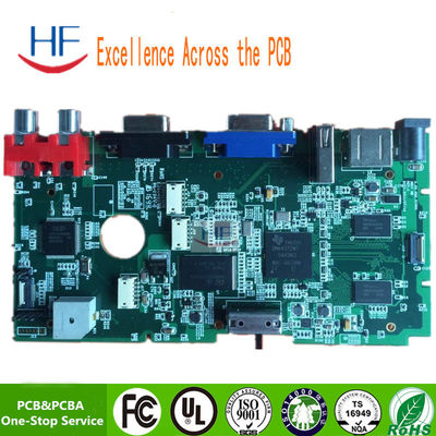
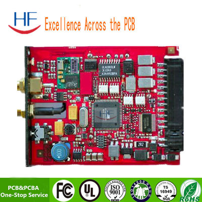
Green 8 Layer HDI 6mil PCB Printed Circuit Board Assembly Design
| 1 | High precision prototype | PCB bulk production |
|
2 |
1-28 layers | 2 layers |
| 3 | 3mil | 6mil |
| 4 | 0.15mm | 0.1mm |
| 5 | Aspect Ration≤13:1 | Aspect Ration≤13:1 |
| 6 | 2 layers:0.2mm;4 layers:0.35mm;6 layers:0.55mm;8 layers:0.7mm;10 layers:0.9mm | 2 layers |
| 7 | Immersion Gold:Au,1—8u” Gold finger:Au,1—150u” Gold Plated:Au,1—150u” Nickel Plated :50—500u” |
Gold Plated:Au,1—150u” |
| 8 | Board thickness≤1.0mm:+/-0.1mm 1.0mm<Board thickness≤2.0mm:+/-10% Board thickness>2.0mm:+/-8% |
1.0mm<Board thickness≤2.0mm:+/-10% |
| 9 | ≤100mm:+/-0.1mm 100< ≤300mm:+/-0.15mm >300mm:+/-0.2mm |
≤100mm:+/-0.1mm |
| 10 | ±10% | ±10% |
Surface mount technology (SMT) assembly process
Compared to the through-hole mounting process, the surface mounting process stands out
in terms of manufacturing efficiency because it has a fully automated mounting PCB
assembly process from solder paste printing, picking and placing, and reflow
soldering.
?Step 1: solder paste printing - apply solder paste to the plate by solder paste
printing machine.The template ensures that the solder paste is left in the correct
position of the mounting element. Also known as the template or solder screen.Since
the quality of solder paste printing is directly related to solder quality, PCBA
manufacturers who specialize in high quality products usually conduct inspections
after solder paste printing by solder paste inspectors.This inspection ensures that
the printing has met regulations and standards.If a defect is found in the solder
paste printing, it must be reprinted or the solder paste must be washed off before the
second printing.
?Step 2: Assembly Installation -- After coming out of the paste press, the PCB will be
automatically sent to the mount machine where the component or IC will be mounted on
the appropriate pad to resist the tension of the paste.The components are mounted on
the PCB board through a component reel in the machine.Similar to the film reel, the
component reel carrying the component rotates to supply the part to the machine, which
will quickly adhere the part to the plate.
?Step 3: Reflow Soldering - After placing each element, the board passes through a 23
'long furnace.A temperature of 500°F will liquefy the solder paste.Now, the SMD
components are firmly bound to the board.
Hybrid technology
With the development of modern science and technology, electronic products become more
and more complex, driving complex, integrated and smaller size PCB board.PCBA with
only one type of component is almost impossible to participate in.
Most boards come with through-hole components and SMD components, which require a
collaboration of through-hole and surface-mount technologies.However, welding is a
complex process that tends to be affected by too many elements.Therefore, it is very
important to better arrange the sequence of through-hole technology and surface-mount
technology.
PCBA using hybrid technology should be performed under the following conditions:
?Single-sided Mixed Components: Single-sided Mixed Components conform to the following
manufacturing procedures: Note: When only a small number of THT components are
required in such components, hand soldering may be used instead of wave soldering.
?Single-sided SMT and Single-sided THT: Note - this type of PCB assembly procedure is
not recommended as adhesives can add to the total cost of PCBA and may cause some
soldering problems.
?Double-sided mixed assembly: In terms of the double-sided mixed assembly method,
there are two options: PCBA with adhesive and PCBA without use.The use of adhesives
increases the total cost of PCB assembly.Moreover, in this PCBA process, heating must
be done three times, which often leads to inefficiency.
Based on the comparison between the mixed assembly procedures described above, it can
be concluded that manual welding is suitable for PCB assembly, which requires many
components on both sides, with more SMD components than THT components.Therefore, wave
soldering is recommended when a small number of THT elements are required.
PCB assembly has to go through such a complex and technical process that many elements
must be carefully considered, and minor modifications can lead to huge changes in cost
and product quality.The description of the PCB assembly process in this article
centers only on typical PCBA programs and techniques.The actual manufacturing process
is largely dependent on the design document and the specific requirements of the
customer.Therefore, how to evaluate a reliable PCB assembler becomes a key issue that
customers must consider before placing a PCBA order.
RFQ
1. Are you headquarter or branch?
We are Ping you headquarter and factory.
2. Can I ask for samples before placing an order?
Yes, we welcome sample order to test and check quality,Miced samles are acceptable.
3. How to be your overseas agent?
Depends which area you are located in,Every conuntries are different.
4. What need I do if I want to pint my own logo?
First, please send us your logo flie in high resolution, We will make some drafts for
your reference to confirm the position and size of your logo.Next we will 1-2 samples
for you to check the actual effect.Finally the formal production will start after the
sample confrimed .
5. Can you ship the goods to my agent or shipping forwarder in China?
Yes,We can,please kindly contact with your agent in advance and us detailed address.
6. How can you solve the problem if receive the defective goods?
Will check all the products before delivery,Please kindly provide the pictures or
video and send back to china or our local agent,After they checking,will replace new
or fix free.